A three-terminal ultraviolet photodetector constructed on a barrier-modulated
triple-layer architecture
Zengxia Mei, Daqian Ye, Huili Liang, Lishu liu, Yonghui Zhang, Junqiang Li, Yaoping Liu,
Changzhi Gu, and Xiaolong Du*
Beijing National Laboratory for Condensed Matter Physics, Institute of Physics,
.Chinese Academy of Sciences, Beijing 100190, P. R. China
Contact e-mail
As we all know, different types of UV photodetectors (PDs) based on ZnO have been
reported early from 1950s; however, they mainly utilize two-terminal devices, such as
photoconductive, Schottky, and p/n-junction. For these structures, there are two critical
drawbacks to be overcome before the applications of ZnO UV-PDs on UV imaging or other
areas: 1) Persistent photoconductivity (PPC) effect, which was extensively ascribed to the
existence of metastable shallow donor state of oxygen vacancy located within the bandgap of
ZnO. Especially under the illumination of short-wavelength light, the PPC can cause the
semiconductor material to remain conductive for hours/days, even in the absence of light. This
increases the response times and limits the frame rates; 2) Low photo gain. A high performance
UV-PDs needs high sensitivity. However, due to the high background carrier concentration and
low photo gain, most UV-PDs suffer from low discrimination ratio between UV and dark/visible
light, which limits the application of UV-PDs
.
We report a novel three-terminal device fabricated on MgZnO/ZnO/MgZnO triple-layer
architecture. Because of the combined barrier modulation effect by both gate and drain biases, the
device shows an unconventional I-V characteristics compared to a common field effect transistor.
The photoresponse behavior of this unique device was also investigated and applied in
constructing a new type UV PD, which may be potentially used as an active element in a UV
imaging array. More significantly, the proper gate bias-control offers a new pathway to overcome
the common PPC effect problem. Additionally, the MgZnO:F as a channel layer was chosen to
optimize the photoresponse properties, and the spectrum indicated a gate bias-dependent
wavelength-selectable feature for different response peaks, which suggests the possibility to build
a unique dual-band UV PD with this new architecture.
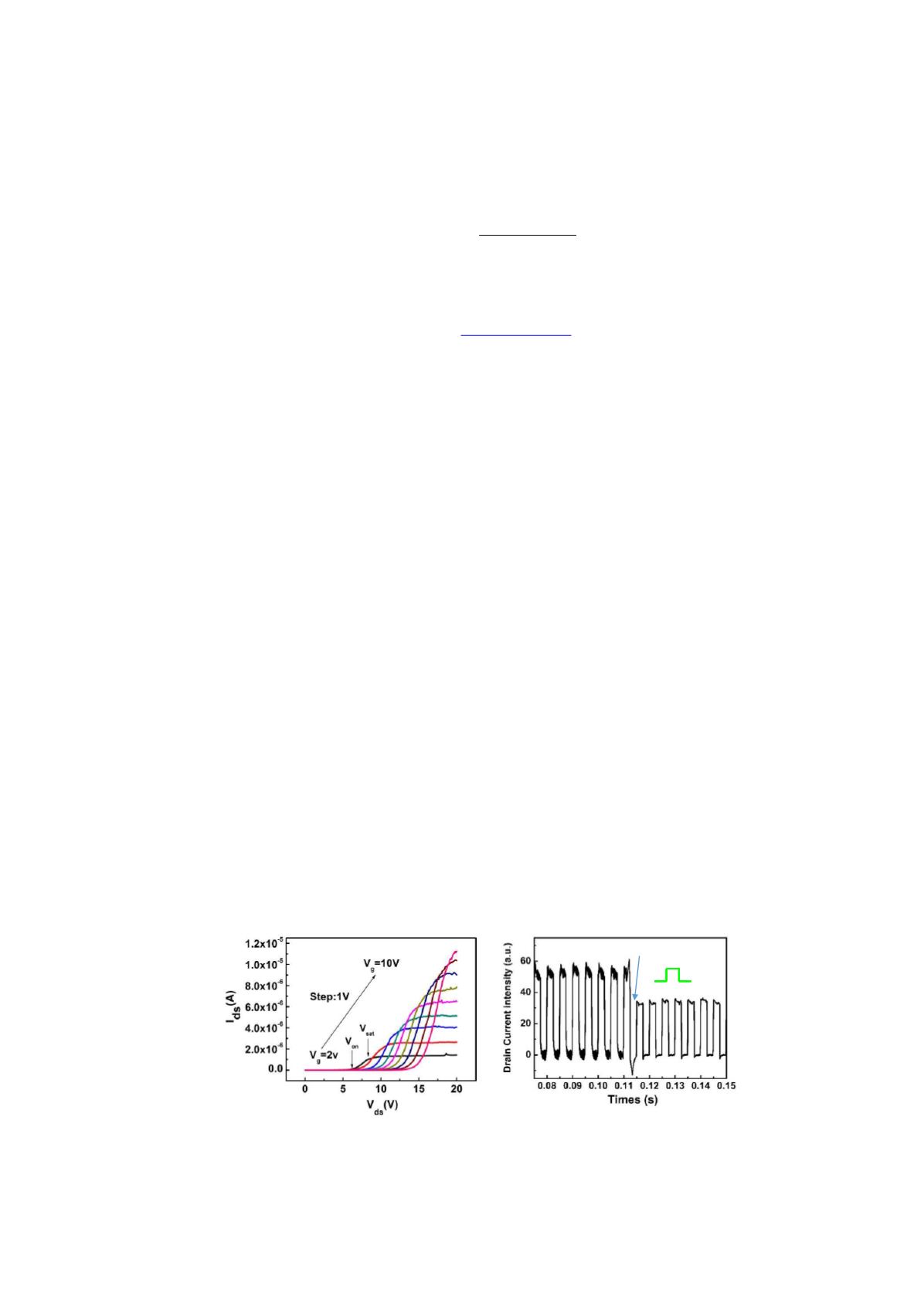
Figure (a) Novel I
ds
-V
ds
characteristics of MgZnO/ZnO/MgZnO/Si FET with V
g
increased from 2 V to 10 V in a forward step of 1V;
(b) Suppression of the PPC when the PD is pulsed with positive gate bias.
Vg=0V
Vg=5V
UV off
(a)
(b)
PS1 7
-163-


