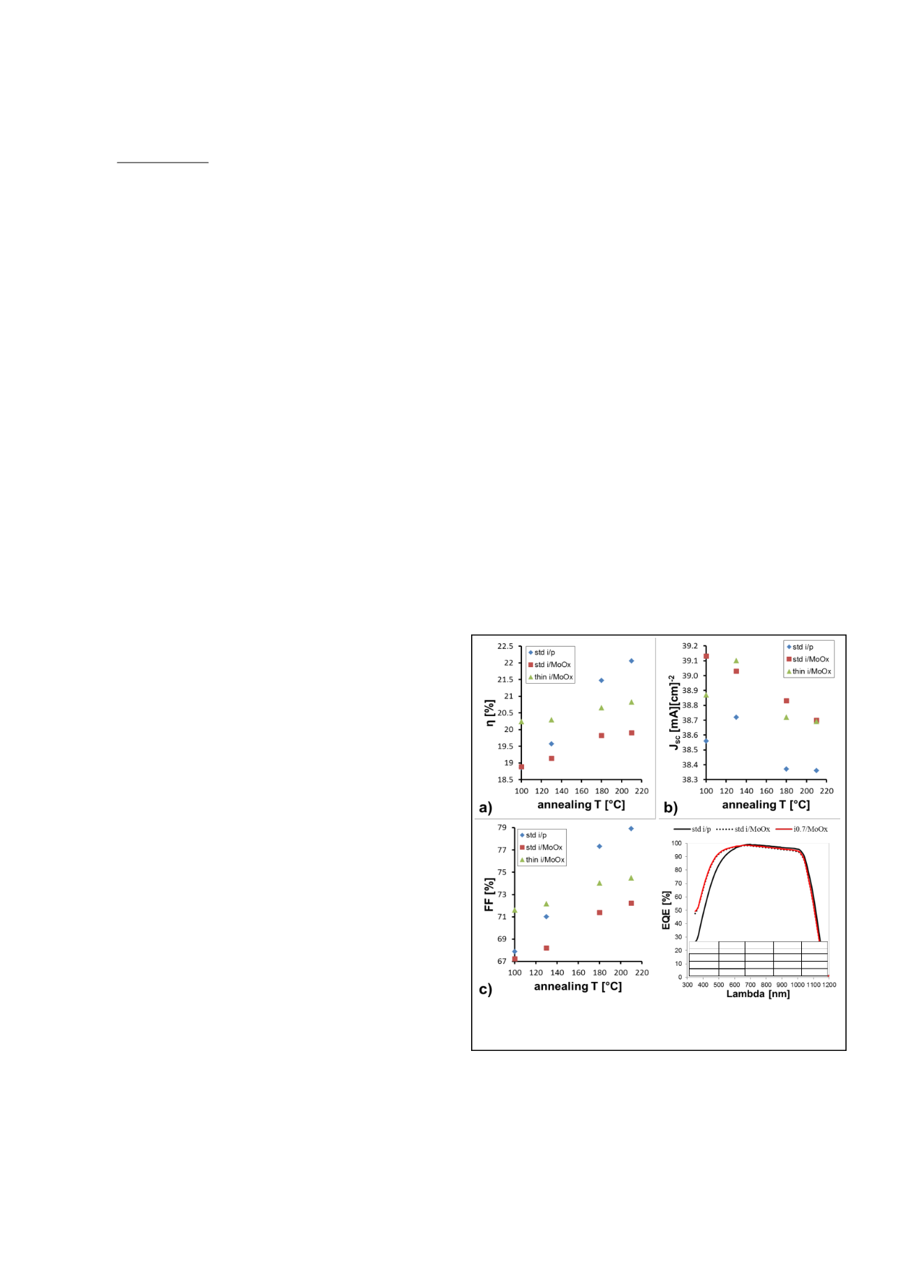
Figure 1: Light J-V curves vs. cumulative annealing temperatures:
(a) Efficiency (b) Jsc (c) FF. In (d) EQE of the devices show
improved UV-Vis response of MoOx cells.
Jsc Jsc_UV Jsc_VIS Jsc_IR
[mA][cm]-2 [mA][cm]-2 [mA][cm]-2 [mA][cm]-2
std i/p
38.40 0.34 32.99 5.07
std i/MoOx 38.70 0.53 33.43 4.74
i0.7 /MoOx 38.70 0.53 33.41 4.76
d)
High efficiency SHJ with MoO
x
carrier selective contact and standard process
D. Sacchetto
1
, G. Christmann
1
, L. Barraud
1
, L. Sansonnens
1
, G. Wahli
2
, A. Descoeudres
1
, N. Badel
1
,
B. Strahm
2
, M. Despeisse
1
, S. Nicolay
1
, and C. Ballif
1
1
CSEM, PV-center, Rue Jaquet-Droz 1, CH-2002 Neuchâtel, Switzerland
2
Meyer Burger Research, Innoparc Rouges Terres 61, CH-2068 Hauterive, Switzerland
In the past decade, silicon hetero junction (SHJ) solar cell technology demonstrated an
ever-increasing efficiency by reducing electrical and optical losses. In that regard, a-
Si:H(i)/a-Si:H(p) passivating layers and the front transparent conductive oxide must be
carefully optimized, as these are the main cause of undesired optical absorption in SHJs. In
the conventional design, the most transparent and conductive front contacts are required to
limit optical losses. Recent implementations exploiting a-Si:H(i)/MoO
x
emitter demonstrated
22.5% efficiency using a low temperature processing and Cu plating (T<130°C) [1]. Notice
however that low cost industrial processing for SHJs exploit higher annealing temperature
both to reduce the screen-printed Ag line resistance and to anneal out the sputtered induced
damage in the i-p layer.
We report here on high efficiency SHJ, using only standard Ag paste metallization with
annealing at temperatures up to 210°C with an optimized a-Si:H(i)/MoO
x
replacement of the
conventional a-Si:H(i)/a-Si:H(p) front contact. We demonstrate that the use of more
transparent a-Si:H/MoO
x
passivating carrier selective contact enables larger photocurrent (
J
sc
of 38.7 mA/cm
2
) leading to an efficiency of 20.7%. Moreover, for the first time we report on
FF improvement with MoO
x
upon annealing with T>130°C, thus enlarging the process
window for MoO
x
.
Interestingly, as shown by LIV measurement in Fig. 1a, at temperatures
T
< 130°C the
efficiency of cells incorporating MoO
x
and thin
a-Si:H(i) layers is effectively superior to that of
reference i/p cells. Such an improvement arises
from a better optical transparency in the UV
and at visible wavelengths, leading to an
increased
J
sc
(see Fig. 1b) which is also
confirmed by EQE (Fig. 1d). Albeit further
curing at higher temperatures leads to an
improved
FF
for all the cells, reference cells
still improve more than MoO
x
-cells (Fig. 1c). In
addition, a thinner layer for a-Si:H(i)/MoO
x
cells show a 2%
FF
gain with respect to the
standard i layer thickness after annealing to
210°C. These different trends lead to a
reference a-Si:H(p)/ITO efficiency of 22% after
annealing at 210°C and to 20.7% with MoO
x
using a thinner a-Si:H(i). Hence we have a first
demonstration of compatibility with standard
industrial processing, but still with strong
potential improvement, in particular in
FF
.
[1] J.Geissbühler, J.Werner, S.Martin de Nicolas, L.Barraud, A.Hessler-Wyser, M.Despeisse, S.Nicolay, A.Tomasi,
B.Niesen, S.De Wolf and C.Ballif. 22.5% efficient silicon heterojunction solar cell with molybdenum oxide hole collector.
Applied Physics Letters, vol. 107, no. 8, page 081601, 2015.
O 62
-136-


