Zinc oxide as indium free transparent conducting oxide for silicon heterojunction solar
cells
G. Christmann
1
, D. Sacchetto
1
, L. Sansonnens
1
, G. Wahli
2
, L. Barraud
1
, A. Descoeudres
1
, B. Paviet-
Salomon, N. Badel
1
, B. Strahm
2
, M. Despeisse
1
, S. Nicolay
1
, and C. Ballif
1,3
1
Centre Suisse d’Électronique et de Microtechnique (CSEM), PV-center, Rue Jaquet-Droz 1, CH-
2002 Neuchâtel, Switzerland,E-mail :
2
Meyer Burger Research, Innoparc Rouges Terres 61, CH-2068 Hauterive, Switzerland
3
École Polytechnique Fédérale de Lausanne (EPFL), Institute of Microengineering (IMT),
Photovoltaics and Thin Film Electronics Laboratory, Rue de la Maladière 71b, CH-2000 Neuchâtel,
Switzerland
Transparent conducting oxides (TCOs) with a high conductivity and low optical absorption
are a key requirement for several applications, and in particular for silicon heterojunction
(SHJ) transparent electrical contacts. Currently, indium tin oxide (ITO) is the industry TCO
reference material thanks to its good properties. However, due to the scarcity and high cost of
indium and the large area required for photovoltaic applications, it is highly desirable to find
alternatives relying on low-cost and more abundant materials. Several alternative materials
have been explored to replace ITO, and among them aluminum doped zinc oxide (AZO)
appears as a good candidate [1]. It exhibits indeed a high bandgap (E
g
= 3.3 eV) ensuring
good near IR, visible, near UV transparency, a reasonably high mobility (>10 cm
2
/(V.s) in
100 nm thin films) and the possibility to be doped up to high carrier concentrations (10
20
‒
10
21
cm
-3
), ensuring good electrical conductivity.
We report here on the use of AZO deposited by sputtering to replace ITO as front and back
contact in SHJ solar cells. Front emitter 2×2 cm
2
test SHJ solar cells were fabricated on 4
inch
n
-type silicon wafers: thin (~10 nm) intrinsic a-Si:H(i) films were deposited by plasma
enhanced chemical vapor deposition on both sides of the wafer for surface passivation. A thin
n-doped a-Si:H film was then deposited to form the back surface field, after that a p-doped a-
Si:H layer was used on the wafer front side to form the hole collector. The transparent
contacts were subsequently deposited by sputtering on
both sides of the cell. AZO was then used either for
front or back contact and compared to reference ITO
material. The cells were finished by sputtering of silver
at the back and screen printing of silver at the front.
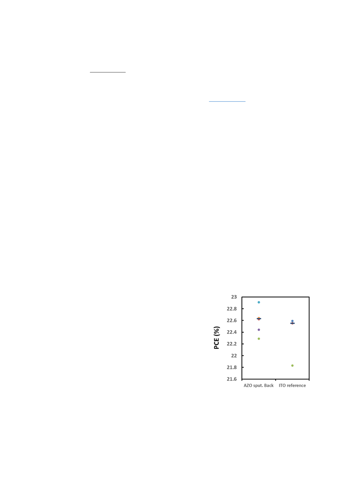
When used as back contact (on
n
-type a-Si:H), AZO
leads to solar cells with efficiencies as good if better
than reference cells (see figure 1). However when used
as a front contact (on
p
-type a-Si:H) AZO leads to
significantly reduced efficiencies. The cells are
characterized by a much lower fill factor than for ITO
ones revealing a poor electrical contact. Strategies for
enhancing this contact and bringing it on par with an
ITO-based one will be presented and the results will be
discussed. Transfer of the results to industrial scale tools will also be presented.
This project has received funding from the European Union’s Horizon 2020 research and innovation programme
under grant agreement No 641864.
[1] K. Ellmer, J. Phys. D: Appl. Phys.
34
3097 (2001)
Figure 1: Peak conversion efficiencies of
SHJ solar cells with AZO back contact
compared to ITO reference
O 42
-104-


